
Si Nanocrystals
Si Nanocrystals (Si-NC) in oxide and nitride matrix are prepared by plasma enhanced chemical vapour deposition (PECVD) or reactive evaporation. The size of the silicon quantum dots is precisely controlled between 2 and 5 nm via the superlattice approach. Due to quantum confinement effects the bandgap of nanocrystalline silicon is increased from 1.1 eV (bulk-Si) up to 1.7 eV. In addition, Heisenbergs uncertainty principle allows for highly efficient radiative exciton recombination (luminescence) in the Si-NCs despite the still indirect bandgap nature. We investigate fundamental physical properties on the nanoscale as well as applications in photovoltaics and optoelectronics.
Preparation of size and density controlled Si nanocrystals
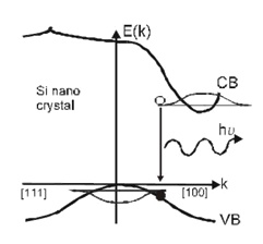 | |
| Transmission electron microscope (TEM) cross section image of a Si nanocrystal superlattice. | Schematic band structure of nanocrystalline silicon [aus: C. Buchal, Physik der Nanostruktur, FZ-Jülich (1998)] |
- Si nanocrystals in a layered arrangement are prepared by depositing Si-rich and stoichiometric dielectric films (e.g. SiOx/SiO2 or SiNx/Si3N4) of nanometer thickness (so called superlattice structure).
- A high temperature annealing (around 1150°C) induces a phase separation of the Si-rich material into Si and the stoichiometric dielectric material. Since a spherical shape minimizes the surface-to-volume ratio the quantum dot diameter can be controlled via the layer thickness. This size control works very well for NC diameters between 5 and 2 nm with Å-precision.
- The excess-Si content determines the areal density of NCs per superlattice layer. Typical values are in the 1012 cm-2 range, corresponding to inter-NC spacings of a few nanometer.
- Excitons (electron-hole-pairs) created by UV excitation are confined in the Si-NCs. Due to the laws of quantum mechanics this results in an increased ground state energy (widening of the bandgap) and an increasing overlap of the electron- and hole-wave function in k-space (Heisenberg) increasing radiative recombination probability.
- Photoluminescence (PL) measurements prove the blueshift of the Si-NC luminescence as function of quantum dot size up to 1.7 eV. The luminescence quantum yield increases to >10%, i.e., by 5 orders of magnitude compared to a bulk Si crystal.
- The luminescence quality of the Si-NC samples is extremely long term stable (no degradation even after many years) since the embedding dielectric matrices are chemically and mechanically very stable.
| (a) Photograph of the PL spectroscopy setup using UV-laser excitation: The laser beam (blue arrow) excites the Si NC sample and the red luminescence is so bright that it is easily observed by the naked eye (red arrow and inset showing a magnification of the sample). (b) The Nanofab PECVD-ALD clustertool (Oxford Instruments Plasmatechnology) used for superlattice deposition. (c) Temperatures beyond 1100°C are used for the Si-NC fabrication. |
Selection of related publications:
M. Zacharias et al., Appl. Phys. Lett. 80, 661 (2002)
J. Heitmann et al., Adv. Mater. 17, 795 (2005)
A. Hartel et al., Thin Solid Films 520, 121 (2011)
Low-temperature properties of Si-NCs
- The investigation of the optical properties down to temperatures of 4 Kelvin gives deep insight into the radiative and non-radiative recombination of excitons.
- Recently, a detailed study reported the systematic blue shift of the size dependent NCs band gap as a function of temperature (4K-300K) and revealed the true origin of a low-temperature PL deviation from bulk Si often observed in literature.
- Our brightly luminescent samples allowed for excitation powers down to the hundred µW/cm² range where the above described effects are not observed anymore. Taking into account the increasing exciton lifetimes in Si-NCs at low temperatures (ms range), the formerly observed PL effects could be ascribed to a simple over-excitation effect, involving double exciton generation and Auger recombination.
- Further work is in progress aiming on a deeper understanding of the recombination mechanisms and the contribution of phonons.
Selection of related publications:
A. Hartel et al., Phys Rev B 85, 165306 (2012)
A. Hartel et al., Phys. Rev. B 87, 035428 (2013)
Investigation of electrical transport and doping of Si-NCs
| Logo of the NASCEnT-project funded within the EU’s 7th framework program (www.project-nascent.eu). |
- Efficient charge carrier transport as well as the ability to introduce majority carriers by doping are considered to be the major obstacles in the implementation of Si quantum dots in photovoltaics. The most prominent idea is the creation of an “all-Si tandem solar cell” where the Si-NCs serve as high bandgap absorber material in the upper cell.
- The superlattice fabrication method allows for the electrical investigation of 3-dimensionally regular Si-NC arrays. In addition, dopants such as phosphorous or boron can be added selectively in the QD-layers during the PECVD process.
- Charge transport between adjacent NCs is generally inhibited due to the highly insulating nature of SiO2 and the huge band edge offsets. If, however, the barriers become as thin as a few nanometers quantum mechanical tunnelling can enable charge transport.
- If a perfectly aligned 3-dimensional array of equally sized NCs is considered, the wave functions of the individual quantum dots can partially overlap which would create so called minibands (in analogy to the “real” energy bands resulting from Bloch's theorem).
- In terms of Si-NC doping fundamental physical questions have to be answered, e.g.:
- Is it at all possible to get impurity atoms in Si-NCs (self purification effects)?
- Do the electronic states of the dopants shift with the quantum confined NC energy states or do they simply create deep levels?
- How do the introduced majority carriers change the electronic and optical characteristics of the Si quantum dots?
- The localization of the dopants and the understanding of their role in the charge carrier transport is currently one of our most important research topics (Reinhard Koselleck Project/DFG and part of the NASCEnT project/EU).
Selection of related publications:
P. Löper et al., Phys. Rev. B 84, 195317 (2011)
S. Gutsch et al., Appl. Phys. Lett. 100, 233115 (2012)
Theses related to Si-nanocrystals:
- Jan Laube: "Silicon Nanostructures: From Isolated Nanocrystals to Percolated Networks", PhD Thesis, Mar. 2018
- Anastasiya Zelenina: "Silicon nanocrystals in various dielectric matrices: Structural and optical properties", PhD Thesis, Nov. 2015
- Sebastian Gutsch: "Electronic Transport in Ordered Silicon Nanocrystal Networks", PhD Thesis, Feb. 2014
- Andreas Hartel: "Structural and Optical Properties of PECVD Grown Silicon Nanocrystals embedded in SiOxNy
Matrix", PhD Thesis, Aug. 2013 - Jan Laube: "Transport Investigastions on Silicon Nanocrystals", Master's Thesis, Apr. 2013
- Rahul Valecha: “Electrical Characterization of Silicon Nanocrystals embedded in SiO2”, Master’s Thesis, March 2012
- Daniel Hiller: “The Influence of Interface Defects on the Optical Properties of Silicon Nanocrystals”, PhD Thesis, May 2011
- Rebecca Michiels: “Determination of Interface Trap Densities on MOS structures using Capacitance and Conductance Measurements”, Bachelor’s Thesis, Sept. 2010
Contact
Dr. Sebastian Gutsch
Nanotechnologie
Georges-Köhler-Allee 103/01/097
79110 Freiburg i. Br.
Tel.: 0761 / 203 - 7258